Half a month ago, on August 9, 2022, President Biden officially signed the Chip and Science Act. Under the $54.2 billion support for the U.S. semiconductor industry, the bill also clearly states: “Subsidized companies cannot make significant expansions in China and related countries in the semiconductor industry for ten years. At the same time, the U.S. has also formed chip alliances with other semiconductor industry powerhouses, such as South Korea, with frequent moves.
U.S. “Chip and Science Act
The future development of China’s domestic chips to replace imported chips has become a foregone conclusion; the relevant industrial applications urgently need development. Hence, water drop laser as the domestic laser cleaning field leader and pioneer, but also in the continuous investment in research and development costs, to explore the possibility of the application of laser cleaning in the chip manufacturing industry, hoping to accelerate the development of China’s semiconductor industry to make their modest contribution.
Wafer cleaning process
In the chip manufacturing industry, semiconductor cleaning, which accounts for more than 30% of the total production process, is a critical process affecting the quality of wafers and chip performance, with a market space of more than 40 billion. Although the importance and equipment market scale is not as crucial as lithography and other core equipment, an irreplaceable link to the chip production yield and the economic benefits of manufacturers have a critical impact.
At present, as the chip manufacturing process continues to improve its level of sophistication, the requirements for the control of wafer surface contaminants continue to improve; after each step of lithography, etching, deposition, and other repetitive processes, a step cleaning process is required, it is certain that the cleaning process is the most frequent of all processes, and will be further increased in the future.
Laser cleaning, as dry cleaning, for the wafer production process of surface contamination – such as dust particles, metals, organic matter, oxides, etc. has a good cleaning effect. Moreover, the accuracy of the effect is more controllable. Still, there are no more mature domestic application examples, water drops laser, to share our wafer surface Roughing process report, hope that the future of laser cleaning can be further involved in the chip manufacturing process.
Wafer Cleaning Report
Cleaning object: Wafer test wafer
Laser cleaning system: Standard laser cleaning system
Customer requirements: remove the wafer surface coverage, and expose the wafer substrate.
Test process.
1) Sample surface state analysis
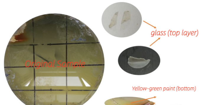
The original surface of the wafer has two layers of coverings; the top layer is transparent glass, and below the glass is a yellow-green paint layer. As shown in Figure 1. There are some unevenly distributed white substances on the edge of the sample.
2) Process window study
Table 1 shows the laser cleaning process parameters used in the test process; figure 2 and Figure 3 are the corresponding macroscopic morphology and microscopic morphology of the laser-cleaned surface under different parameters, respectively.
By optimizing the laser cleaning process parameters, the wafer surface coverage needs to be cleaned in layers three times, the first time using TS1 parameters to remove the glass layer on the wafer surface, the second and third time using TS2 parameters to remove the paint layer on the wafer surface.
Experimental process using higher power parameters, try to remove the wafer surface covering layer by cleaning two times process, found that it is unable to clean or damage the wafer substrate phenomenon, the current experiment by three times the best cleaning effect.
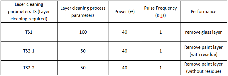
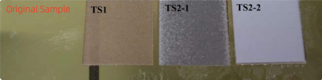
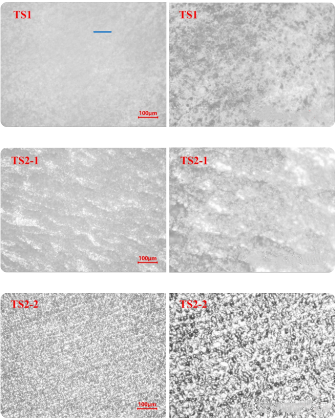
Figure 3 shows the microscopic appearance of the wafer surface after laser cleaning with different process parameters; after laser cleaning with TS1 parameters, the glass layer on the sample surface is completely removed to reveal the bottom layer of the lacquer. After laser cleaning, further testing is required to determine whether the wafer surface condition meets the production requirements.
Laser cleaning, an emerging industrial cleaning technology in China, has not yet heard of practical applications in the production process of wafers. But the initial cleaning tests can be seen, and laser cleaning in the semiconductor field is still promising, just before no one has made the preliminary technical attempts. Therefore, we will further explore the possibility of laser cleaning in the chip manufacturing application later to help develop China’s semiconductor industry.